Semiconductor
High-performance solutions designed, built, and integrated to reduce waste and optimize efficiency for semiconductor manufacturers.
Our systems deliver high-performance solutions designed, built, and integrated to ensure optimum results for all your precision manufacturing challenges.
Key Applications
- Wafer handling/processing
- Wafer (de)lamination
- Fan-out technology
- Via inspection
- Die attach
- Inkjet nozzle plate
- Probe cards
- Custom wafer metrology
- Build-to-print
Technologies
- Precision assembly and automation
- Advanced material handling
- Vision systems


Ready To Get Started?
Advanced Solutions for Semiconductor

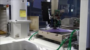
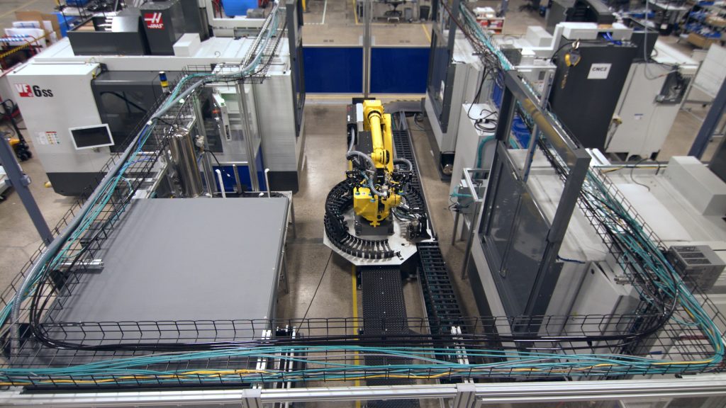
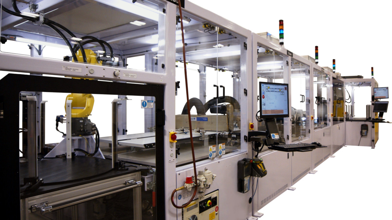
Our systems designed for the semiconductor industry are characterized by configurable, modular work cells that perform a variety of assembly tasks, including part installation and removal, fastener insertion and removal, CNC machining, defect detection, inspection, and testing. Using a modular design, systems are customizable to each project’s specific needs. Systems typically include input tray handling and bulk feeding of parts, vision-guided part insertion and removal, ultrasonic welding, laser marking, 6-axis robots with custom end-effectors, conveyance and buffer integration, color and defect detection, and packaging.

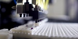
Silicon wafers require very precise systems to perform metrology, defect detection, dispense, and assembly operations. Our wafer metrology and assembly systems can detect and measure features on silicon wafers with accuracies down to 1μm using high-performance, high-resolution vision systems and laser interferometers. For assembly operations, our systems use vision systems to align components and apply 150μm adhesive dots to silicon wafers with 20μm accuracy.
Using technologies designed for parallel processing, our carefully engineered systems correctly assemble defect free products faster than 50 parts per minute using ceiling mounted robots to reduce overall floor space and high intensity lighting to obtain the best image contrast. By automating assembly and inspection processes, our clients improve manufacturing yield from 70% with manual inspection to 99% using advanced machine vision.
Success Stories
Polishing Pad Inspection System
A semiconductor manufacturer needed an automated system to clean and inspect polishing pads for semiconductor wafers.
Precision Adhesive Dispensing System
A semiconductor manufacturer needed a fully automated system to dispense precise quantities of adhesive to predefined areas on a customer-supplied wafer.
